Semiconductor Device & Assembly Manufacturing 7/21/26
Semiconductor Device & Assembly Manufacturing US/EU
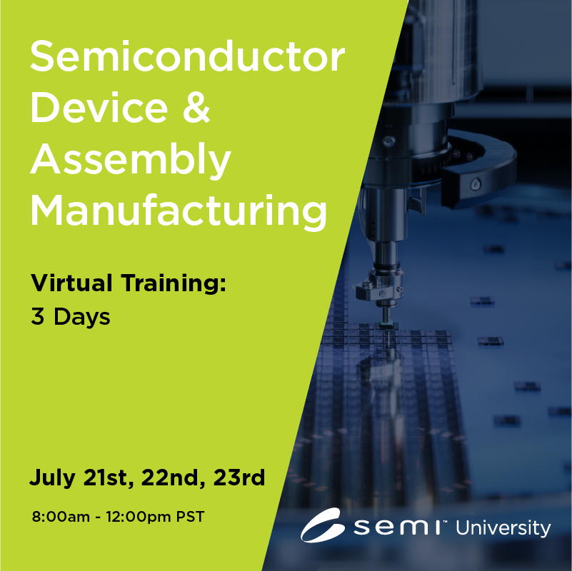
Dates & Times
July 21st - July 23rd
8:00 AM– 12:00 PM PST
Location
Webinar
Pricing
Early Bird $100
Members: $799 $699
Non- Members: $849 $749
The Semiconductor Device and Assembly Manufacturing workshop is a 12-hour webinar that is held for 4 over three days. This three-day workshop provides a complete overview of the semiconductor manufacturing process. The class focuses on key process steps needed to form a functioning device. Some important science and engineering ideas needed to understand device manufacturing will be discussed. The workshop is designed for non-technical personnel needing an understanding of fab process steps. Some technical background from attendees will improve the workshop learning.
The first day will overview the fab process steps with a brief summary of how a transistor functions. We will discuss how multiple transistors are connected to form a logic or memory device. We will also cover how a transistor works with respect to the physical layout of Bipolar and MOSFET transistors.
Day two will cover key fab process steps. Ion implantation, photolithography including DUV and EUV processes, plasma processes including deposition and etch, rapid thermal processing, and wet etch processing. Specific emphasis will be given to the different wet etch processes.
The third day of the workshop will focus on the new transistor designs, including FinFET and CFET designs. We will also cover reasons for changing the transistor design and newer materials, including tantalum, hafnium, silicon germanium, and low-k dielectrics. We will also review roadmaps of leading companies, including TSMC, Intel, and Samsung.
After completing the workshop, the student will be able to describe all fabrication and assembly process steps and understand how these steps work together to form the completed integrated circuit, as well as future structures.
By focusing on a Do It Right the First-Time approach to the analysis, participants will learn the appropriate methodology to successfully locate defects, characterize them, and determine the root cause of failure.
Who Should Attend
Process Technician
Material Engineers
Process Engineers
Equipment Manufactures
Technical Marketing Engineers
-
Anyone wanting to learn more about semiconductor devices and assembly manufacturing
Course Topics
Silicon wafer manufacturing
Basic operating principles of transistors and semiconductor devices
Planar, FinFET, and GAA transistor formation and design differences
-
Fab processes needed to form a semiconductor, including the following:
Lithography, with a focus on DUV and EUV methods
Etching, including wet and plasma processes
Deposition, thermal, plasma, electroplating deposition
CMP and modern CMP processes
Cancellation and Rescheduling Policies
· Registrants may cancel or reschedule a class no less than 30 days before the class start date.
· Cancellations received after the stated deadline will not be eligible for a refund.
· Cancellations will be accepted via email to semiu-support@semi.org
· All refund requests must be made by the registrant or the credit card holder.
· Refund requests must include the name of the attendee, the course name, and the date of the session.
· Refunds will be credited to the original payment method used for payment.
· SEMI reserves the right to cancel any course due to low enrollment or other circumstances that would make the event unavailable 7 business days before the class's start date.
· If SEMI cancels a class, the registrants will be offered a full refund.
This product has no reviews yet.