Back-End of Line Assembly Processes
Course Description
The semiconductor industry provides critical enabling technology for many products and fields and has seen periods of rapid growth. While electronic goods dominate the market, communications, medical devices, and the automotive industry show signs of increased potential.
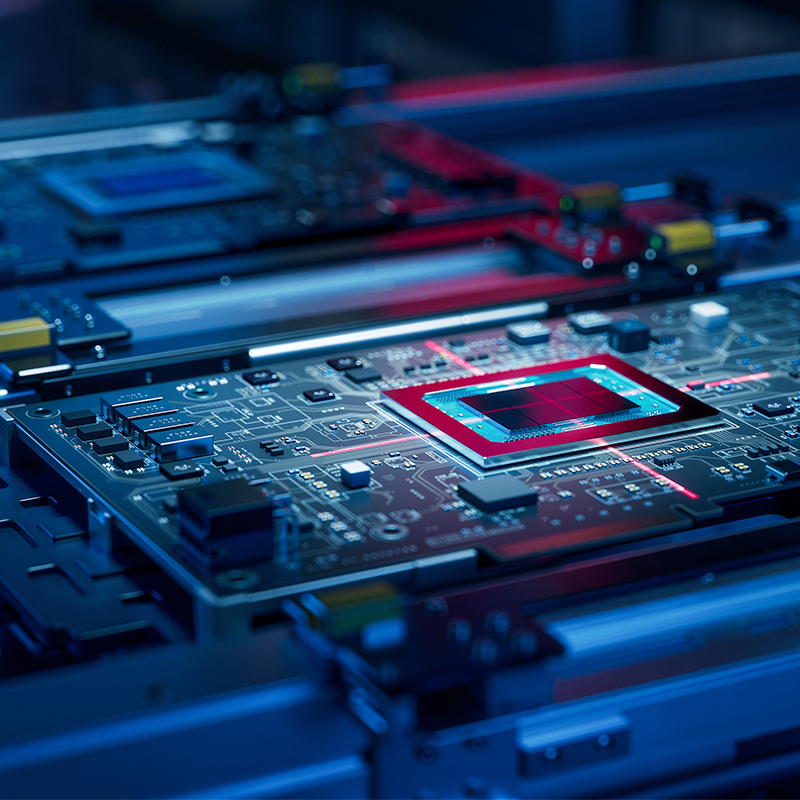
This course provides an overview of end-of-line packaging assembly. As different packages have different assembly processes, this course touches on key package assembly technologies for wirebond leadframe packages and flip chip on substrate packaging. Key assembly processes of molding, underfilling, plating, ball attach, and PCB assembly will be shared in this course. Those interested in end-of-line assembly will learn about these technologies, inclusive of their various processes, materials, and future direction to meet the semiconductor application needs.
Learning Objectives:
Explain the properties of mold compound affecting package reliability.
Describe the underfill and encapsulant of flip chip technologies.
Identify plating parameters related to the plated surface.
Describe the formation of the intermetallic effect of ball attachment.
Explain the surface mount technologies in PCB assembly.
Course Duration
75 minutes
Target Audience
Sales engineers/business development executives, college students who are interested in joining the semiconductor industry, especially in OSAT, EMS, and IDM (Package Assembly.) Materials and equipment from industry companies can take advantage of this curriculum to ensure their workforce is ready.
Requisite Knowledge
At least some college-level scientific knowledge
This product has no reviews yet.