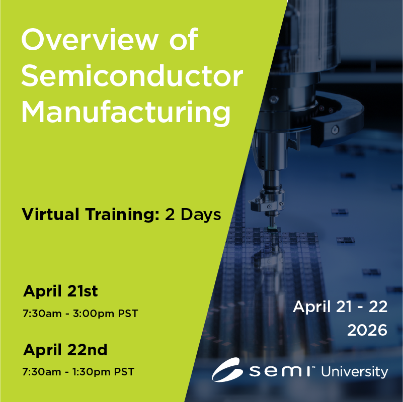
Overview of Semiconductor Manufacturing Americas 04/21/26
Gain a comprehensive understanding of the semiconductor industry and manufacturing process, design, and ecosystem of the semiconductor industry.
Understand the jargon, tools, and materials used in the design and fabrication of an integrated chip.
Effectively be able to communicate semiconductor manufacturing concepts with other associates and industry professionals.
Basic Electronics and Microelectronics: Definitions of essential electronic terms/concepts and introduction to microelectronics and integrated circuits.
Process nodes: Process nodes and their impact on device performance and cost
Device physics and transistor operation: Principles of device operation and transistor functionality
Crystal growth and wafer prep: Crystal growth techniques and wafer preparation processes
Advanced Transistor Technologies: FDSOI, FinFets, and gate all around (GAA) transistors and their impact on device performance.
Circuit design and layout: Introduction to circuit design, layout techniques, and tools.
-
Wafer Processing:
Mask-making techniques and materials used in lithography: Techniques & materials used in mask-making & various lithographic methods (DUV, Immersion, EUV)
Clean Room Environments: Importance of clean rooms in semiconductor manufacturing. and contamination issues.
Etching & Cleaning Processes: Plasma & wet etching processes
Ion Implantation and & Diffusion Techniques: Methods for doping & controlling diffusion in semiconductor fabrication.
Deposition Techniques: RTP, CVD, AVD, & ALE techniques & their effect on device performance.
Electroplating & Sputtering: Metal deposition techniques used in manufacturing.
Packaging & Testing: techniques such as wire bonding, die stacking, flip chip, & chiplets packaging, and semiconductor testing processes.
Metrology & Measurement Tools: Tools & methods used for precision measurement in semiconductor manufacturing.
Semiconductor Industry Ecosystems: Learning the major players in the industry
This product has no reviews yet.