Overview of Semiconductor Manufacturing Asia 09/30/2025
Overview of Semiconductor Manufacturing Webinar Asia
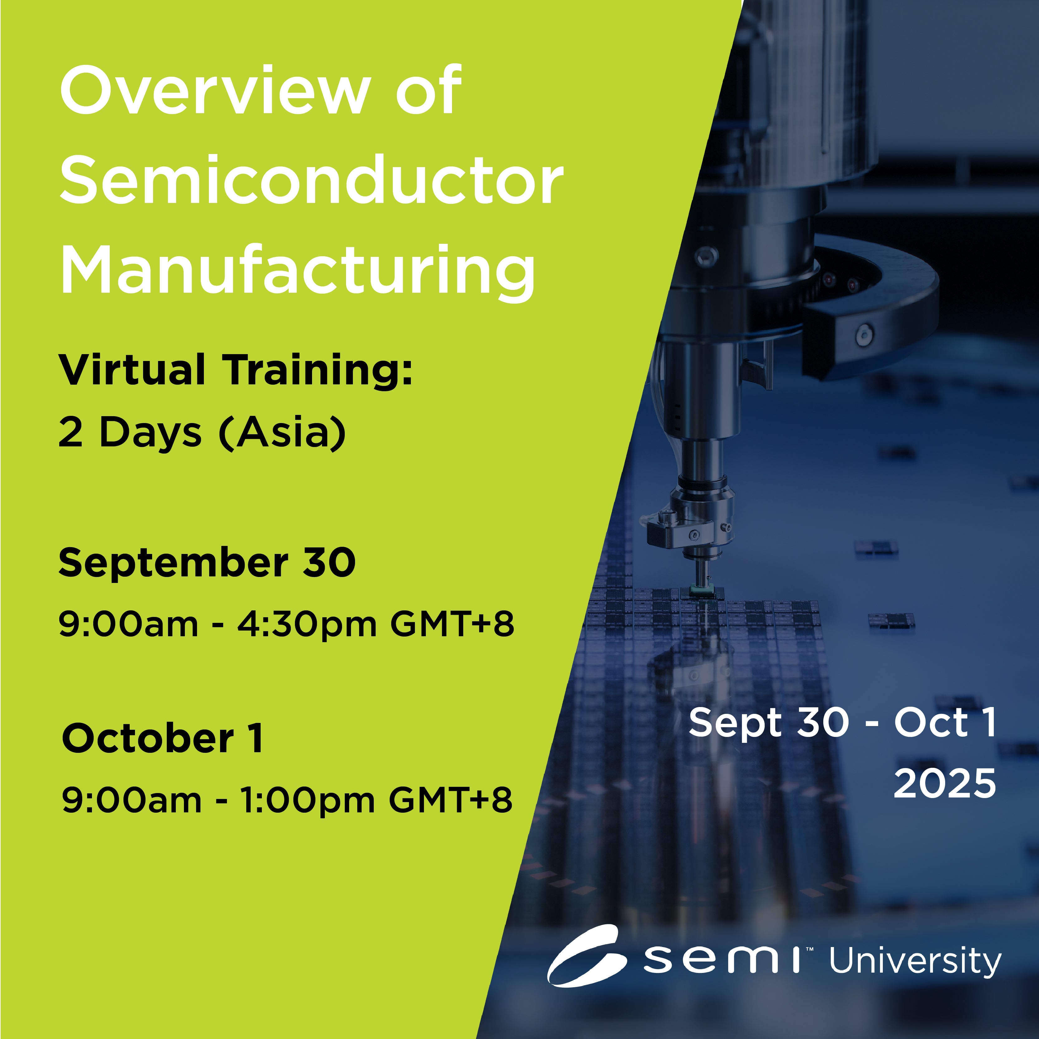
2 Days
September 30th and October 1st, 2025
Dates & Times
September 30th & October 1st
Asia
9:30 AM– 4:30 PM GMT +8 (Day 1)
9:30 AM – 1:00 PM GMT +8 ( Day 2)
Location
Virtual
Pricing
Members: $895 $795
Non-Members:$995 $895
This course offers a solid foundation in semiconductor manufacturing, from basic concepts to advanced techniques, providing practical insights into the tools, processes, and technologies driving the industry.
Learning Objectives:
- Gain a comprehensive understanding of the semiconductor industry and manufacturing process, design, and ecosystem of the semiconductor industry.
- Understand the jargon, tools, and materials used in the design and fabrication of an integrated chip.
- Effectively be able to communicate semiconductor manufacturing concepts with other associates and industry professionals.
Course Topics:
- Basic Electronics and Microelectronics: Definitions of essential electronic terms/concepts and introduction to microelectronics and integrated circuits.
- Process nodes: Process nodes and their impact on device performance and cost
- Device physics and transistor operation: Principles of device operation and transistor functionality
- Crystal growth and wafer prep: Crystal growth techniques and wafer preparation processes
- Advanced Transistor Technologies: FDSOI, FinFets, and gate all around (GAA) transistors and their impact on device performance.
- Circuit design and layout: Introduction to circuit design, layout techniques, and tools.
-
Wafer Processing:
- Mask-making techniques and materials used in lithography: Techniques & materials used in mask-making & various lithographic methods (DUV, Immersion, EUV)
- Clean Room Environments: Importance of clean rooms in semiconductor manufacturing. and contamination issues.
- Etching & Cleaning Processes: Plasma & wet etching processes
- Ion Implantation and & Diffusion Techniques: Methods for Doping & controlling Diffusion in Semiconductor Fabrication.
- Deposition Techniques: RTP, CVD, AVD, & ALE techniques & their effect on device performance.
- Electroplating & Sputtering: Metal deposition techniques used in mfg.
- Packaging & Testing: techniques such as wire bonding, die stacking, flip chip, & chiplets packaging, and semiconductor testing processes.
- Metrology & Measurement Tools: Tools & methods used for precision measurement in semiconductor mfg.
- Semiconductor Industry Ecosystems: Learning the major players in the industry
This course is suitable for anyone seeking a better understanding of the semiconductor industry, market leaders, terminology, business, and the semiconductor ecosystem.
Cancellation and Rescheduling Policies
· Registrants may cancel or reschedule a class no less than 30 days before the class start date.
· Cancellations received after the stated deadline will not be eligible for a refund.
· Cancellations will be accepted via email to semiu-support@semi.org
· The registrant or the credit card holder must make all refund requests.
· Refund requests must include the attendee's name, Course Name, and session date.
· Refunds will be credited to the original payment method used for payment.
· SEMI reserves the right to cancel any course due to low enrollment or other circumstances that would make the event unavailable 7 business days before the class's start date.
· If SEMI cancels a class, the registrants will be offered a full refund.
If you have any questions, please reach out to us at semiu-support@semi.org
This product has no reviews yet.