Semiconductor Manufacturing I
Course Description
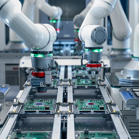
Semiconductor manufacturing is a complex process involving many steps. This course covers two crucial steps in the manufacturing process: silicon wafer fabrication and semiconductor deposition. The silicon wafer fabrication step encompasses single-crystal growth, wafer grinding, wafer slicing, wafer edge grinding, wafer lapping, wafer etching, and wafer polishing. The semiconductor deposition step includes various important types of deposition processes in semiconductor manufacturing. To enhance the learning experience, the course contains interactive quizzes, allowing learners to test their knowledge and retention of visually engaging content.
Learning Objectives
• Describe the various steps involved in the fabrication of silicon wafers, including crystal growth, slicing, lapping etching, and polishing.
• Recognize the types of epitaxy and the process involved in creating them.
• Identify the different types of deposition processes used to create thin films and patterns on silicon wafers, and the application of each method.
• Explain the basic principles of the different types of deposition processes, such as CVD, PVD, ALD, ECD, and SOD.
Course Duration
2 hours
Target Audience
Quality, manufacturing, engineering, designing, testing, purchasing, and sales functions at organizations that require an understanding of how semiconductor devices are manufactured.
This product has no reviews yet.